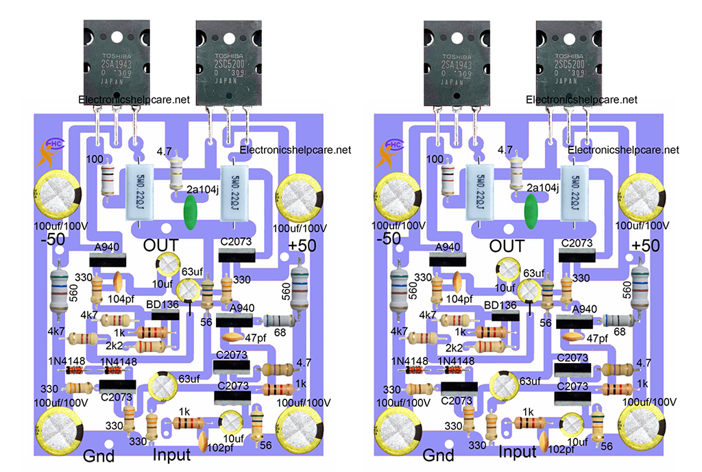
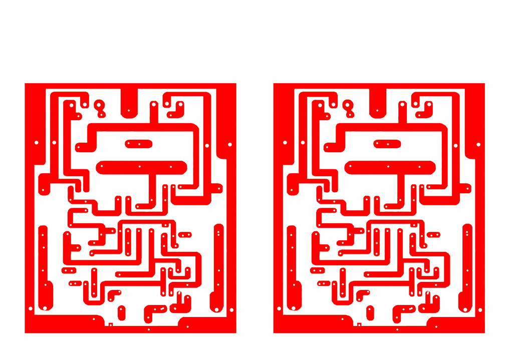
Stereo amplifier circuit diagram:
This is the Stereo amplifier circuit diagram. in this board, we can use 20-0-20 voltage to a maximum of 50-0-50. this board can make 150 watts. if we use 50-0-50 voltage then we have to use 3 amperes. here used 2sc5200 and 2sa1943 transistors. These pair transistors can make 150 watts.

Details about 2SC5200
2sc5200 Polarity is NPN. Max Collector Power Dissipation is 150 Watts. The Max Collector-Base Voltage is 250 Voltage. Max Collector-Emitter Voltage is 250 Voltage. The Max Emitter-Base Voltage is 5 Voltage. Maximum Collector Current is 17 amperes.
Details about 2SA1943
2sa1943 Polarity is PNP. Max Collector Power Dissipation is 150 Watts. The Max Collector-Base Voltage is 250 Voltage. Max Collector-Emitter Voltage is 250 Voltage. The Max Emitter-Base Voltage is 5 Voltage. Maximum Collector Current is 17 amperes.
Here we can see that the maximum voltage is 250, which can throw the Emitter and Collector. The base can take 5 voltages. and the voltage ampere can take a maximum of 17.

This circuit doesn’t have speaker protection. here, we need a speaker protection circuit. here is the link to get the speaker protection circuit. Diagram is here
This is the Speaker protection circuit diagram. It can protect our Speaker from the burn. if the amplifier has any problem then this circuit can save our soundbox. Normally when the transistor makes a short circuit the voltage comes out from the speaker output line then this circuit protects that voltage. This circuit should not allow any direct voltage to be sent to the speaker. This circuit is essential for protecting the speaker.
We have another post for you. like Stk 4101 repairing amplifier,
Build a Transformer or construct the transformer. Home Theater Circuit Diagram 5.1
Thanks a lot for being with us. If you want another post then please visit our website.
We have another post for you. like repairing amplifiers, If you like electronics please visit our other post. electronicshelpcare.com
our Facebook page is Electronicshelpcare
 Electronics Help Care electronics circuit diagram


